题目内容
(请给出正确答案)
题目内容
(请给出正确答案)
[多选题]
Sequential logic circuits can be divided into the following three main categories:()
A.Event Driven
B.Clock Driven
C.Power?Driven
D.Pulse Driven
提问人:网友lixin080108
发布时间:2022-01-07
题目内容
(请给出正确答案)
B.Clock Driven
C.Power?Driven
D.Pulse Driven
 更多“Sequential logic circuits can …”相关的问题
B.Sequential logic circuits require a means by which events can be sequenced,while combinational logic circuits do not neeD
C.Combinational logic circuits are perfect for situations when we require the immediate application of a Boolean function to a set of inputs, however, sequential logic circuits to change its value with consideration to its current state as well as its inputs.
D.Combinational logic circuits are perfect for situations when we require the immediate application of a Boolean function to a set of inputs, so do sequential logic? circuits.
A.Sequential logic circuits require a means by which events can be sequenced,so do combinational logic circuits.
B.Sequential logic circuits require a means by which events can be sequenced,while combinational logic circuits do not neeD
C.Combinational logic circuits are perfect for situations when we require the immediate application of a Boolean function to a set of inputs, however, sequential logic circuits to change its value with consideration to its current state as well as its inputs.
D.Combinational logic circuits are perfect for situations when we require the immediate application of a Boolean function to a set of inputs, so do sequential logic? circuits.
Analyze sequential logic circuit in the following figure. Write down the Excitation Equation, Next State table. Draw the State convert table and verify whether the circuit could be self-starting. Start with an initial state of 100. 分析下图中的时序逻辑电路。 写出驱动方程,画出状态转换表,校验电路是否可以自启动。
A.directly
B.immediately
C.instantly
D.snapshot
Analyze the following sequential logic circuit, its function of the circuit is (______). 如下时序逻辑电路功能是(______)。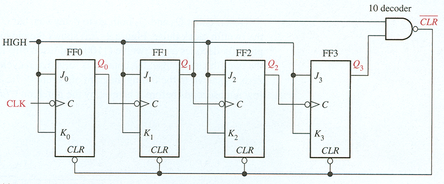
A、A Moore type synchronous Modulus-10 Counter 摩尔型同步10进制计数器
B、A Mealy type asynchronous Modulus-11 Counter 米利型异步11进制计数器
C、A Moore type asynchronous Modulus-10 Counter 摩尔型异步10进制计数器
D、A Moore type asynchronous Modulus-11 Counter 摩尔型异步11进制计数器
A、123
B、231
C、321
D、312
(2) 3D Heterogeneous Integration Every logic generation needs to add new functions in each node to keep unit price constant (to preserve margins). This is getting more difficult due to the following challenges: • Little functions left on board/system to co-integrate • Heterogeneous cores specialized per function—specialized performance improvement requirements needed per each dedicated core • Off-package memories—costly to co-integrate with logic, technology not fitting to baseline CMOS (where wafer/die-level stacking might be needed) Die cost reduction has been enabled so far by concurrent scaling of poly pitch, metal pitch, and cell height scaling. This would like to continue until 2024. Cell height scaling would likely to be pursued by 3D device (e.g., finFET and lateral GAA), device stacking, 3DVLSI, and design-technology-co-optimization (DTCO) constructs in cell and physical design. However, this scaling route will become challenged by diminishing electrical/system benefits and also by diminishing areareduction/$ at SoC level. Therefore, it is necessary to pursue 3D integration routes such as device-over-device stacking and/or monolithic 3D (or sequential integration) These pursuits will maintain system performance and power gains while maintaining the cost advantages such as treating expensive non-scaled components somewhere else and using the best technology fit per tier functionality. 3DVLSI offers the possibility to stack devices enabling high-density contacts at the device level (up to 100 million vias per mm² with N14 ground rules). 3DVLSI can be routed either at gate or transistor levels. The partitioning at the gate level allows IC performance gain due to wire length reduction while partitioning at the transistor level by stacking nFET over pFET (or the opposite), enabling the independent optimization of both types of transistors (customized implementation of channel material/substrate orientation/channel and raised source/drain strain, etc.) while enabling reduced process complexity compared to a planar co-integration, for instance the stacking of III-V nFETs above SiGe pFETs. These high mobility transistors are well suited for 3DVLSI because their process temperatures are intrinsically low. 3DVLSI, with its high contact density, can also enable applications requiring heterogeneous co-integration with high-density 3D vias, such as NEMS with CMOS for gas sensing or highly miniaturized imagers. In order to address the transition from 2D to 3DVLSI, the following generations are projected in the IRDS roadmap: • Die-to-wafer and wafer-to-wafer stacking o Approach: Fine-pitch di-electric/hybrid bonding and/or flip-chip assembly o Opportunities: Reducing bill-of-materials on the system, heterogenous integration o Challenges: Design/architecture partitioning • N&P stacking o Approach: Sequential integration o Opportunities: Reducing 2D footprint of standard cell o Challenges: Minimizing interconnect overhead is key between N&P enabling low-cost • Adding logic 3D SRAM and/or MRAM stack (embedded/stacked) o Approach: Sequential integration and/or wafer transfer o Opportunities: 2D area gain, better connection between logic and memory enabling system latency gains. o Challenges: Solving the thermal budget of interconnect at the lower tier if stacking approach is used, Revisiting the cache hierarchy and application requirements, power, and clock distribution • Adding Analog and I/O o Approach: Sequential integration and/or wafer transfer o Opportunities: Giving more freedom to designer and allows integration of high-mobility channels, pushing non-scaling components to another tier, IP re-use, scalability, IO voltage enablement in advanced nodes o Challenges: Thermal budget, reliability requirements, power and clock distribution • True-3D VLSI: Clustered functional stacks, beyond CMOS adoption o Approach: Sequential integration and/or wafer transfer o Opportunities: Complementary functions other than CMOS replacement such as neuromorphic, highbandwidth memory. Application examples include image recognition in neuromorphic fabric and wideIO sensor interfacing (e.g., DNA sequencing, molecular analysis). o Challenges: Architecting the application where low energy at low frequency and highly-parallel interfaces could be utilized, mapping applications to non-Von Neumann architectures. 1) Which of the following may not be the challenge to add new functions in each node of logic generation? () A Little functions left on board/system to co-integrate B Heterogeneous cores specialized per function—specialized performance improvement requirements needed per each dedicated core C Technology not fitting to baseline CMOS D SRAM and FLASH memories 2) Which of the following may not reduce the die cost? () A Scaling of pecialized performance B Scaling of poly pitch C Scaling of metal pitch D Scaling cell height 3) Cell height scaling would likely to be pursued by () A 3D device B Device stacking C 3DVLSI D all of the above 4) 3D integration routes may not include () A device-over-device stacking B scaling of poly pitch C sequential integration D monolithic 3D 5) We can maintain the cost advantages by () for 3D integration. A using new materials for channel B using high κ dielectrics for gate C treating expensive non-scaled components somewhere else D Moore’s Law 6) According to the author, which of the following is false? () A 3DVLSI may achieve high-density contacts at the device level. B 3DVLSI can be routed either at gate or transistor levels. C 3DVLSI allows IC performance gain due to wire length reduction D 3DVLSI may enable the optimization of one type of transistors. 7) What is the challenge for monolithic 3D integration? () A Design of the system B Architecture C Minimizing interconnect overhead D Applications requiring heterogeneous co-integration with high-density 3D vias 8) What is the advantage of the N&P stacking? A Reducing bill-of-materials on the system B Reducing 2D footprint of standard cell C Reducing the thermal budget of interconnect D All of the above 9) According to the author, which of the following can achieve the 2D area gain? () A Logic 3D SRAM and/or MRAM stack B Scaling of poly pitch C Scaling of metal pitch D All of the above 10) The author implies that neuromorphic may () A be realized by wafer transfer. B be realized by CMOS solution. C be used in Von Neumann architectures. D be a highbandwidth memory.


为了保护您的账号安全,请在“简答题”公众号进行验证,点击“官网服务”-“账号验证”后输入验证码“”完成验证,验证成功后方可继续查看答案!

 微信搜一搜
微信搜一搜
 简答题
微信搜一搜
简答题
简答题
微信搜一搜
简答题

 如搜索结果不匹配,请